Founded in 1987, TSMC is a pure-play semiconductor foundry. Foundries package their manufacturing processes in a Process Design Kit (PDK), which gives customers a defined interface while protecting proprietary process recipes. With a PDK, chip companies can outsource manufacturing and focus on design. Companies that follow this model are known as fabless firms.
Will the division of labor in the design process also change?
NovaSilicon (Shanghai Xinxingyuan Intelligent Technology Co., Ltd.) calls its approach a Circuit Design Kit (CDK). It packages chip-design expertise and AI agents into a system. From chip specifications to GDS layout, the implementation process that requires repeated iterations is done by NovaSilicon engineers using CDK. NovaSilicon says it originated the CDK concept. The company calls this proposed division of labor “Designless”: chip companies would specify what they need, while CDK-supported engineering teams handle implementation.
Regarding CDK, the company recently released two papers that put the two Agent systems in CDK and general Agents such as GPT-6 Astra on the same set of questions. Including analog layout design and digital chip layout planning (floorplan).
The highest average scores for both scenarios come from NovaSilicon's self-developed Agent system designed based on CDK: the simulated layout is 0.8154 points (GPT-6 Astra is 0.7483 points); the floorplan is 57.97 points, which is approximately 1.9 times that of GPT-6 Astra.
In the five months since its establishment, NovaSilicon has raised hundreds of millions of yuan in three consecutive rounds of financing. The latest round of financing was led by Shunwei Capital, followed by GGV Capital and Matrix Partners. Previously, NovaSilicon has received investment from Wuyuan Capital, SenseTime Guoxiang Capital, Shanghai Future Industry Fund, Shanghai Science and Technology Innovation Group and other institutions.
Since its establishment, NovaSilicon has quickly gathered and trained many composite engineers and researchers with experience in both AI and chip design.
First mention of CDK: PDK in the design process
NovaSilicon's idea is to do what foundries have done in the design process. In this analogy, AI agents and simulators are production equipment, CDK provides the process recipes, chip specifications are the input, and the output is a GDS layout.
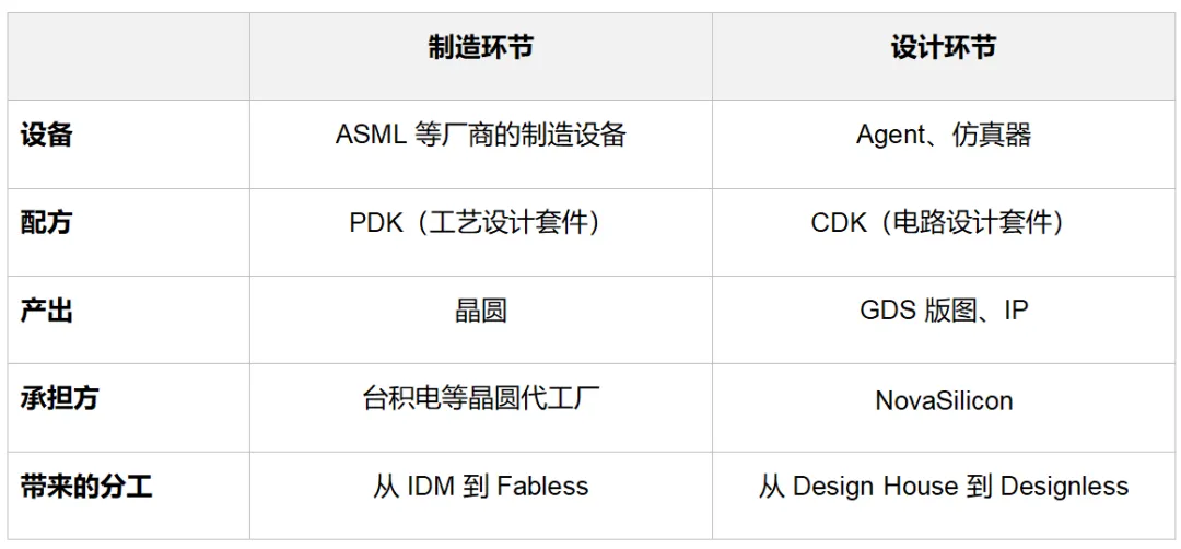
Table 1 | Comparison of PDK and CDK. Source: NovaSilicon
Designless extends the fabless division-of-labor model. The chip company defines the specification, and CDK and its engineering teams handle implementation. NovaSilicon positions CDK as a model-driven AI-IC design system. Chip design experience is accumulated in the Design Kit, not in large models or EDA tools.
Analog direction CDK Vega covers topology selection, netlist to schematic, device size, simulation and layout. Digital Direction CDK Sirius, including design initialization, floorplan, place and route, clock tree, physical verification and timing analysis on the back end, specification understanding, modeling, RTL generation and verification on the front end.
Each of the two papers tested one link. The simulated layout article tested Novara in Vega, and the floorplan article tested Nova-SI in Sirius.
- Paper 1: AnalogLayoutWorld: An Open Benchmark for Agentic Analog Layout Design
- Paper 2: Evaluating AI Agents for Industrial-Level Chip Floorplanning: A Framework and Empirical Study
- Author: Nova-Silicon Team
Paper link: [https://arxiv.org/abs/2611.12048,https://arxiv.org/abs/2611.16991]
General Agent draws simulation layout: 91.1% handed in the paper, 21.3% passed the acceptance test
The benchmark of the first paper is called AnalogLayoutWorld.
Layout is the last step in analog chip design. The circuit engineer first determines the transistor-level netlist, which is equivalent to a wiring list, indicating which devices are used, how large they are, and how they are connected to each other. The layout engineer then draws the construction drawing according to it, draws each device as a geometric figure on the silicon wafer, arranges the position, connects the metal lines, and outputs a GDS file that can be handed over to the wafer factory.
AnalogLayoutWorld has 40 tasks covering amplifiers, references, power management circuits, sampling circuits, and oscillators. The Agent gets the fixed netlist and electrical indicators for layout design, and the score depends on six items: whether the GDS is handed over, LVS (whether the layout and netlist are consistent), DRC (whether the process rules such as line width and spacing are met), area compactness, engineering quality, and whether the post-simulation is up to standard. Engineering quality is defined by the team and analog layout engineers, examining device matching, key signal routing and power supply.
There is an acceptance line beyond the score. Acceptance is considered only if DRC, LVS and all post-simulation conditions have passed, and the aspect ratio and shape of the layout are also qualified.
The team tested 13 combinations of general models and Agent frameworks, and CDK: Novara in Vega also ran through the same set of questions.
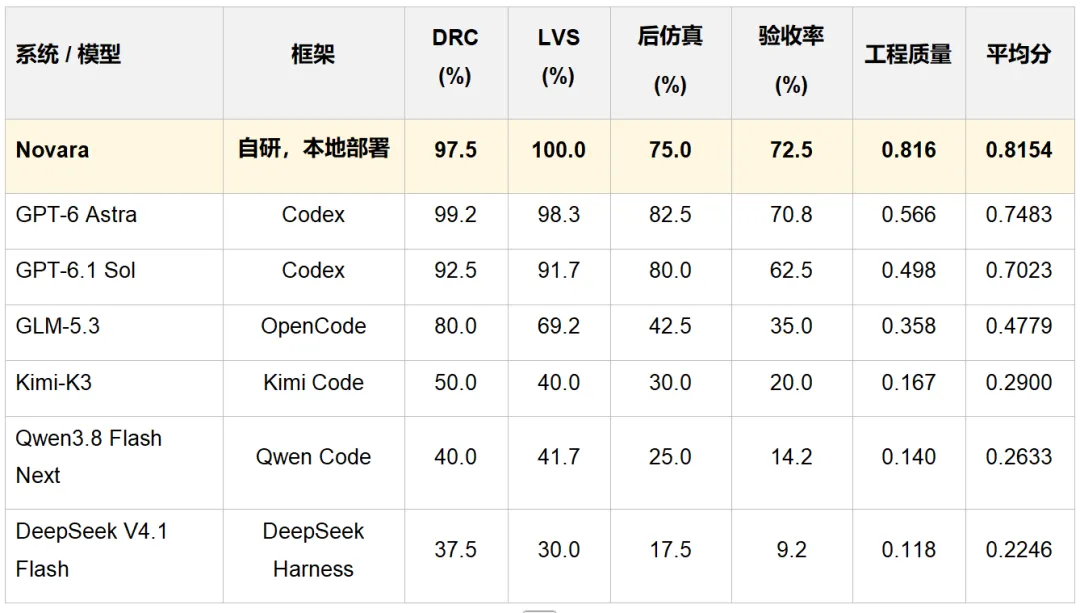
Table 2 | AnalogLayoutWorld main results (excerpt). Data source: Paper Table 1
Novara ranks first with an average score of 0.8154. The acceptance rate is 72.5%, which is also the highest. The average score of GPT-6 Astra is 0.7483, with an acceptance rate of 70.8%. GPT-6.1 Sol is 0.7023 and 62.5%. The average scores for the two configurations of GLM-5.3 range from 0.46 to 0.48, with the remaining configurations scoring less than 0.30.
Novara’s LVS pass rate is 100%. In terms of engineering quality, Novara scored 0.816, and the second-ranked GPT-6 Astra scored 0.566.
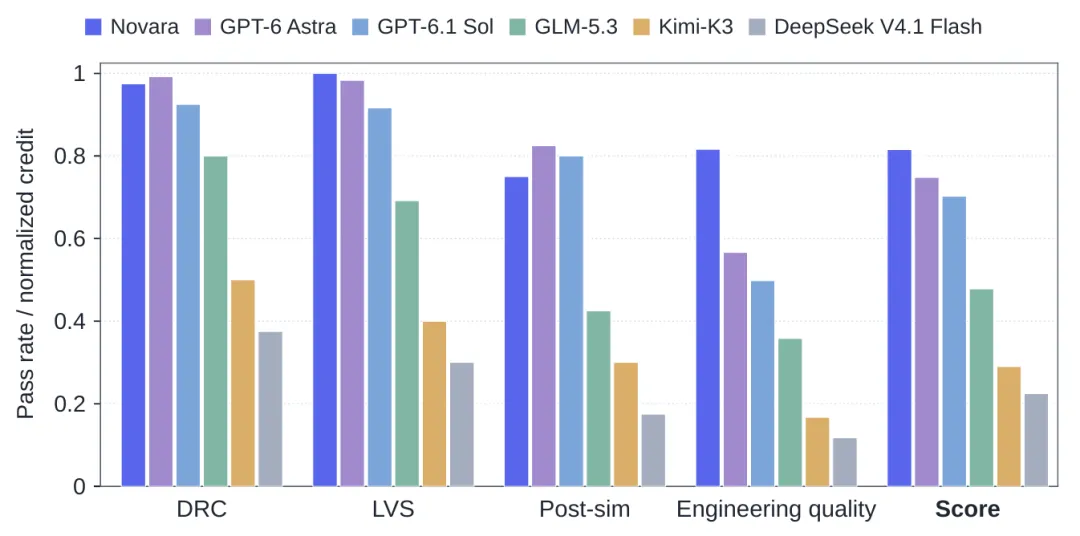
Figure 1 | Comparison of Novara and five common Agent configurations. DRC, LVS, and Post-sim are the passing rate, and Score is the average score of the 40 questions. Source: paper
GPT-6 Astra's post-simulation pass rate is 82.5%, which is higher than Novara's 75.0%, but the acceptance rate is only 70.8%. The paper explains that the lost parts of the GPT series between simulation and acceptance are mainly due to the unqualified aspect ratio and shape of the layout. Novara ranges from 75.0% to 72.5%, and the layout that has passed the simulation can basically be accepted.
The simulation passed, but GPT handed over a 209 micron thin strip.
Question 40 includes a current-starved ring VCO. GPT-6 Astra passed DRC, LVS and two post-simulations in all three attempts, but the layout delivered was about 209 µm wide, less than 10 µm high, with an aspect ratio between 22.63 and 26.31, and the upper limit specified by the evaluation was 4. Such a slender strip is difficult to integrate with the surrounding circuitry, and it only received 0.3 points three times.
From the track record, Astra first tried folding a long resistor in the circuit. As a result, the folding scheme failed to match the length parameter of LVS, so it returned a 203.19 µm long straight resistor and lined up the remaining devices along the resistor. This is a typical behavior of pursuing rigid indicators while ignoring the needs of the real analog circuit tape-out level.
For the same question, Novara's first attempt produced a layout of 34.14 × 42.33 µm, an aspect ratio of 1.24, and a score of 0.9015. Novara pays more attention to modeling that conforms to the layout design ideas actually used by engineers, and also obtains layout results that are closer to engineering use.
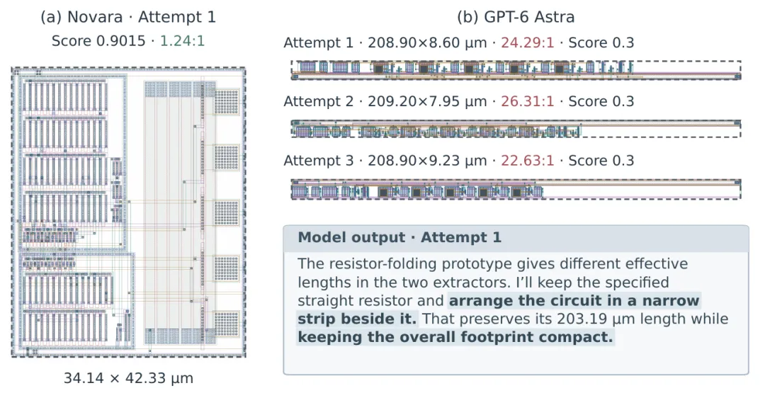
Figure 2|Four layouts of a circular VCO. The left is Novara’s first attempt, and the right is GPT-6 Astra’s three attempts. All four passed DRC, LVS and post-simulation. Source: paper
Industrial design with 99 hard macros: about 1.9x that of GPT-6 Astra on average
The second paper switched to the digital chip backend and tested floorplan.
When a digital chip changes from a logical netlist to a physical layout, the first step is to decide where to place the large modules. These large modules are called hard macros, which have a fixed shape and cannot be scaled. After the hard macro is placed, the EDA tool fills in the remaining space with standard cells and connections. Intuitively speaking, this is like deciding on the location of dozens of buildings on a piece of land, leaving the remaining land for small houses and roads. If the building is not well arranged and the total area is sufficient, some roads will still be blocked.
The paper uses an industrial design: 235,727 instances, 99 hard macros occupy 71.1% of the 14.123 mm² layout area, and the largest and smallest hard macro areas differ by about 121 times. The board area is L-shaped, and the missing corner cannot be used.
The evaluation connects the hard macro layout handed over by the Agent to a prescribed downstream process: building power and ground networks, making standard cell layouts, estimating global wiring, and analyzing setup time. The total score of the evaluation is out of 100, which is obtained by multiplying congestion, timing, wire length and standard unit utilization. The evaluation system is divided into three groups. The first group is Nova-SI, which is self-developed by NovaSilicon and deployed locally. The second group is a general engineering agent that can query the design database, call EDA tools, and get feedback from downstream processes before making modifications. The third group only has file read and write permissions.
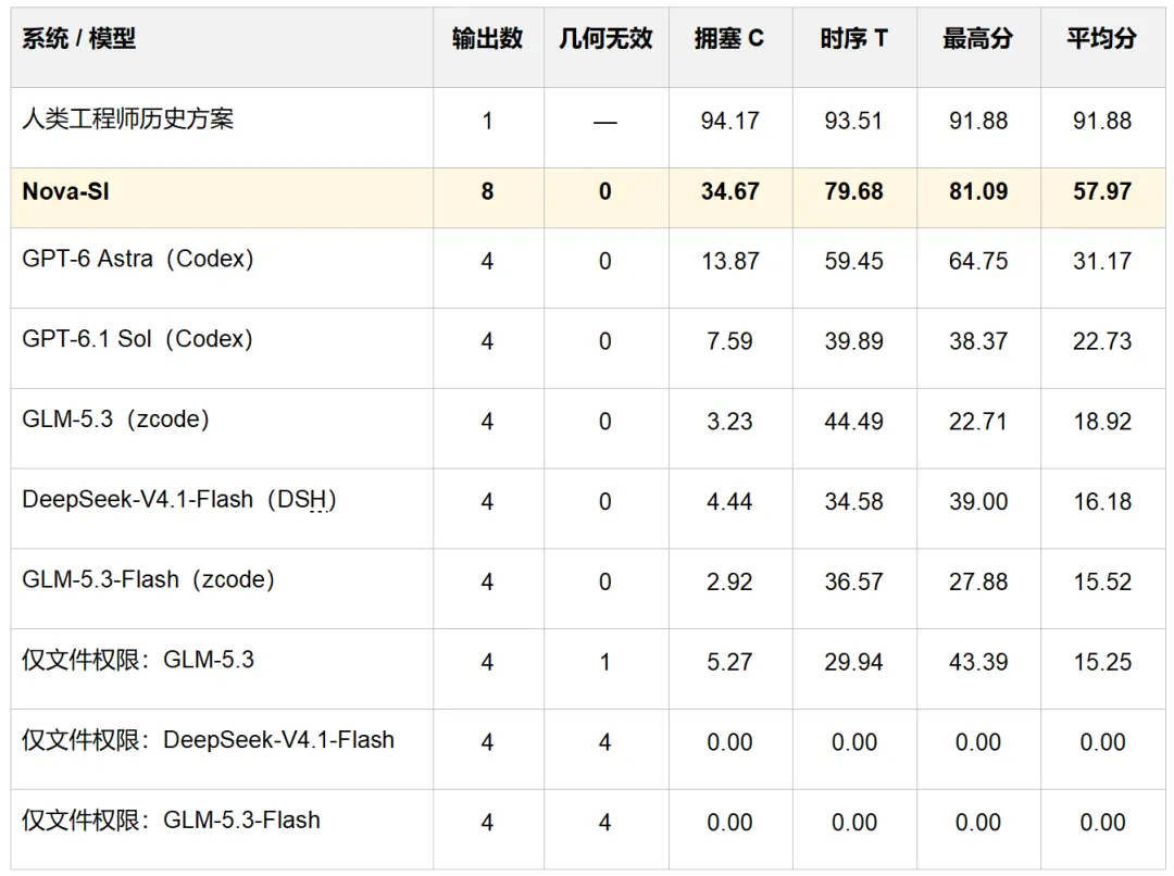
Table 3|floorplan evaluation results. Each item is worth 100 points, and invalid geometry and delivery failure will be worth 0 points. Data source: Paper Table 1
The average score for Nova-SI is 57.97, GPT-6 Astra is 31.17, and the remaining common configurations are between 15 and 23. For the group with only file permissions, 9 of the 12 outputs had hard macros that crossed the boundary or overlapped, and were scored 0 points. All eight Nova-SI outputs passed the geometry check, with a median score of 57.52. Astra's median score is 21.37 points, with 3 out of 4 outputs falling below Nova-SI's lowest score. When formulating the plan, Nova-SI did not use the online feedback of the prescribed process. The general group where Astra is located can call EDA at any time to see the results and then make changes. In terms of token consumption, Nova-SI outputs an average of 36.13M per copy, and the five configurations of the general group range from 62.11M to 286.50M.
Excluding Nova-SI's best output, the mean is 54.67. The paper multiplied each of the seven rating scales by 0.5, 1, and 2, and tried 2,187 combinations. The average value of Nova-SI was 22.30 to 30.38 points higher than Astra. The highest score among the 8 outputs is 81.09 points. For reference, the historical solution for this design by human engineers is 91.88 points.
Figure 3|The layout with the highest score of Nova-SI (No. 07, 81.09 points), from left to right are hard macro, standard unit and congestion heat map. Source: paper
The future of CDK
CDK was first used in NovaSilicon's own design process. Based on CDK, NovaSilicon currently serves chip design companies and customers with IP needs. There are two first batch directions. One is to use the UCIe PHY IP being developed by Vega. UCIe is the industry standard for chiplet interconnection, and PHY is the physical layer interface. The other is the design service of 3D integrated computing (CIM) chips, and digital design CDK, Sirius, has been used in this service.
Large model manufacturers are equipment manufacturers that provide the underlying base for CDK, which is as important as the lithography machines used by TSMC. However, just as PDK and recipes are core to supporting TSMC in changing the semiconductor industry, CDK will also reshape the semiconductor industry from Fabless to Designless.
NovaSilicon introduces Design Kit from process manufacturing into the design process. The company expects this model to scale as semiconductor manufacturing has, opening a new path for scaling chip-design work.